|
| ||||||||||||||||||||||||||||||||||||||||||||||
|
Section: Science Life |
deutsche Version  Print-Version |
|
Nanotechnology Centre "FIRST Lab" In the realm of the smallest | |
|
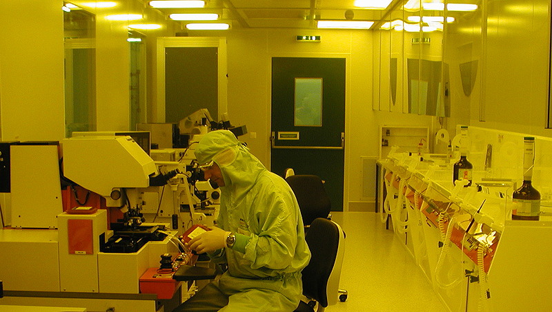
Not all branches of technology strive towards ever bigger and ever more spectacular constructions. Interest in the art and finesse of precision on minute scales has continued to grow since the production of the first microchips. ETH Life visits "FIRST Lab" at Hönggerberg a year after its inauguration. By Christian Thalmann It could easily be taken for a secret laboratory. No arrows of direction, no posters, no maps call attention to its existence. Granite and whitewashed cement keep silent. The cool, sterile corridor is no different from any other in this building. It seems, Iif one does not know the way, one does should not need to know. An emergency shower off the stairwell hints at the danger of chemical accidents. Only a big nameplate next to a door in the corridor announces the Clean Room Centre FIRST. FIRST stands for "Frontiers In Research: Space and Time". The name highlights the technological challenges that plaster the route leading to all kinds of ever smaller, ever quicker construction elements. The aim of this 30 million franc project is to give ETH a platform that conforms to the very latest standards of technology for research and development in the micro and nanosciences. Since its inauguration in summer 2002 (1) the lion’s share of work hours has been invested in the installation, testing and starting up of new equipment. Nothing stands now in the way of research. A big to-do for a bit of air The entire top floor of FIRST Lab is taken up with equipment that assures the delivery of water, electricity, heat, pressure, gas (including gases of the poisonous and explosive sort), liquid nitrogen and other resources to the clean rooms below. Hundreds of sensors constantly monitor this network and set off the alarm if they detect anything untoward. In every room pressure, humidity and temperature are kept as constant as possible. The be-all and end-all of clean rooms is the air circulation. All laboratories are continuously fed with minutely filtered air, which flows through the ceiling from air ducts near the floor of the service room into which all laboratories are embedded. This technology guarantees a consistent, unperturbed top down circulation (what experts refer to as a laminar flow), which reduces dust particle concentrations to an absolute minimum. Obviously, open hair, woolly jumpers and dusty shoes are not welcomed here. All staff and visitors have to dress up in clean room overalls and shoes before entering. Even scribbling on everday notepads counts as contamination; only guaranteed fibre-free clean room paper is allowed.
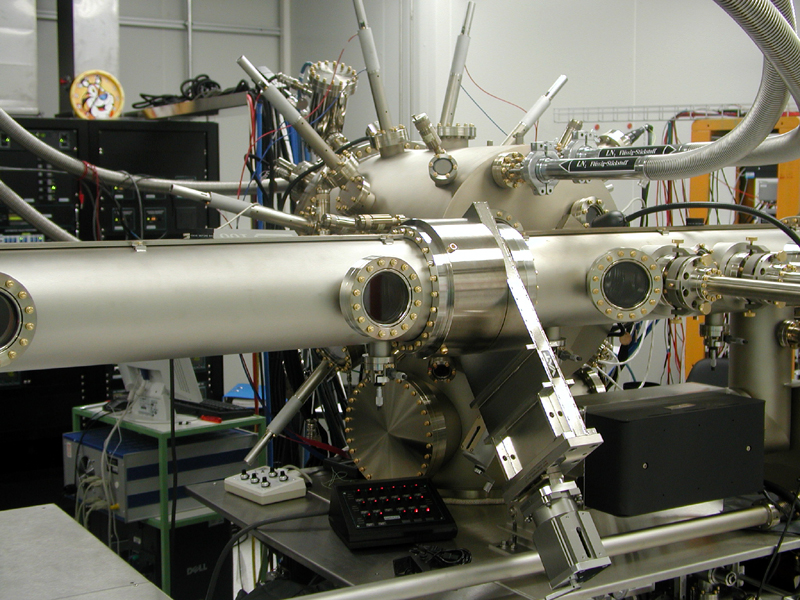
Coating under extreme conditions The basic material for the nano structures being developed in the lab is a thin, monocrystalline wafer made of a III-V-semiconductor material. In an epitaxial reactor layers of metal or doped semiconductors are applied to the wafer. Optical means, electronic diffraction and an atomic force microscope are used, amongst other tools, to check the thickness, structure and electrical band gaps of the application. The required high levels of purity and precision calls for the use of a so-called molecular beam epitaxy. In a brassy gleaming behemoth of a stainless steel vacuum chamber the reactants are split into single atoms or molecules and shot onto the wafer. To avoid contamination from other elements this takes places in a ultrahigh vacuum. "The background pressure in the reactor is held at 10 to the power of minus 11 millibars," explains Dr. Dirk Ebling. "That is 10,000 times thinner than the vacuum surrounding the International Space Station." The initial materials, such as Ga, Al, In or As etc., also have to be available in an extremely pure form. "With a purity of 99,9999% an otherwise relatively worthless element can be worth more than commercial gold."
|
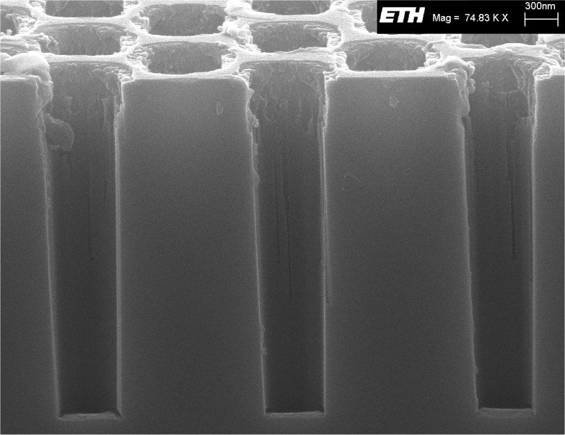
Batik methods in mini format It is not easy to get a high concentration of integrated circuits, electronic construction elements and nanostructures on to a chip, especially one aims at an efficient manufacturing process. This is where photoresist comes into play. The wafer is coated with a thin film of this light-sensitive resin and a reticle,of the desired structure is laid over it. The wafer is then exposed to ultraviolet rays. In those places where the reticle does not cover it, the photoresist undergoes a chemical change and becomes susceptible to a certain solvent. This means that the coat of photoresist can be selectively removed, there. After that the reticle is removed and a metal layer, for example, is steamed on. Another solvent now eliminates the layer of photoresist that was not exposed to rays together with its metal layer the metal only remains in the places where it lay directly on the substrate. One is left with a metal structure that exactly corresponds to the reticle. The photoresist method not only makes it possible to produce precise structures on the substrate, but can also be employed to etch precise holes or channels. In a crystal lattice the etching speed of acid on the direction, and this can have either desired or destructive consequences. For this reason chemical etching is an art, and scientists at FIRST Lab have already reached high levels of proficiency. If one wants to make do without such effects, etching can also be carried out with a directional plasma, so-called "dry etching". The size of things to come The laboratory is currently working on a number of projects within which the concepts of "ever smaller" and "ever faster" stand at the centre of optical, electrical or acoustic devices, such as for instance the construction of mirrors with special absorbers that enable laser pulses of femtoseconds or less. For fast data communication one needs amplifiers and switches; for this purpose, users of FIRST are developing transistors with communication speeds of 100 GB/s and optical switches with switching times of under 1ps. Sufficient integration density of optical construction elements is a great problem, and this problem is being attacked with the development of suitable structures with photonic crystals. Ever higher integration density calls for structures that descend to atomic dimensions, in extreme cases ones that enable switching processes using single electrons. Some projects are investigating the physical characteristics of structures at this level by producing quantum devices, for example, or SET (Single Electron Transistors). Acoustic devices on micro and nanoscales are also being developed with similar methods in order to use them, for example, as fast switching devices or filters. Further questions dealing with the realms of micro and nanotechnology, such as thermoelectric generators or interactions between biological materials and semiconductors, will be addressed in future projects.
|
|||||||
|
Footnotes:
You can write a feedback to this article or read the existing comments. | ||||||||